NEUTRONOPV - New neutron techniques to probe bulk heterojunction solar cells with graded morphologies understanding the link between processing, nanostructure and device performance
Gabriel Bernardo, Andrew J. Parnell, David Lidzey, Stephen M. King, Richard A. L. Jones
PART I
Small Angle Neutron Scattering (SANS), despite being a technique that has been around for several decades and that has contributed greatly to the development of soft-matter science, has been absent from most of the developments in the
study of the morphology of bulk-heterojunction (BHJ) solar cells, performed over the last two decades. Although some SANS studies have been previously performed in these conjugated-polymer:fullerene systems, they were mainly based on
thick solvent-cast films and not in thin films as used in functioning organic photovoltaic (OPV) devices. Therefore, in this project the most important objective was to develop the potential of SANS for studying the morphology of thin
films as used in real BHJ solar cells, as an exemplar of the emerging classes of functional organic and hybrid devices which are expected to have significant economic and societal impact in coming decades.
The methodology adopted, in order to generate good signal to noise statistics in the SANS signal, consisted in assembling thin BHJ films deposited in quartz windows into stacks (typically between 12 and 18 windows per stack) and placed
inside specially designed aluminium sample holders as shown in Figure 1 below.
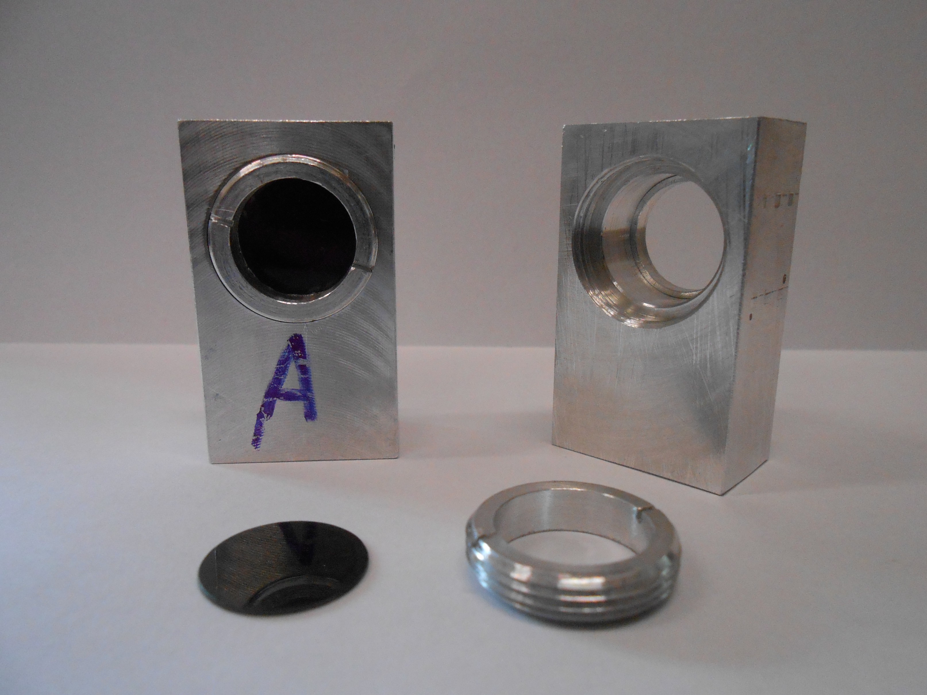
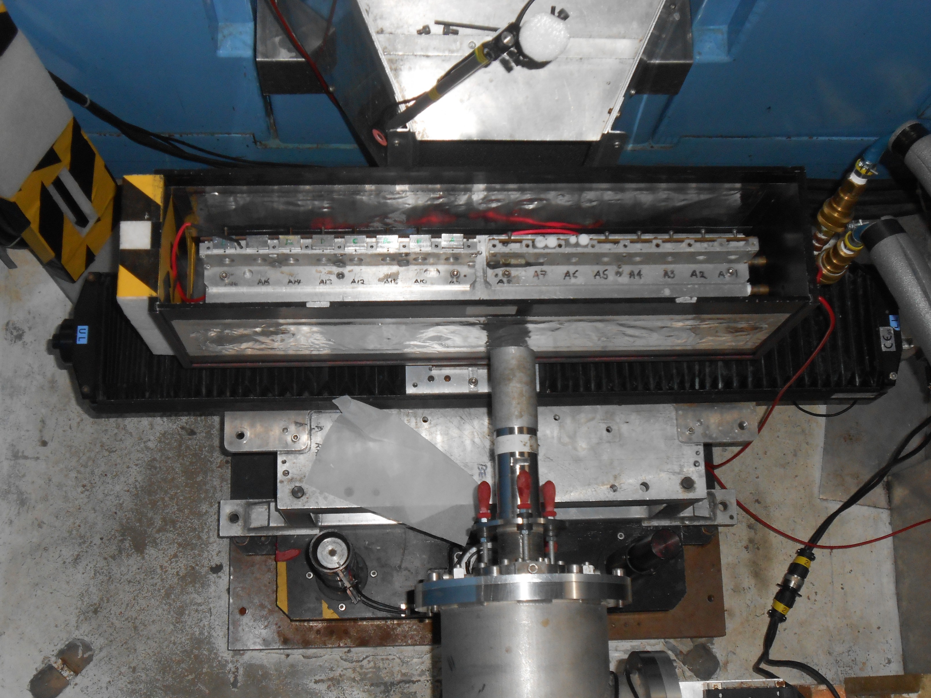
Figure 1. (Left) Aluminium sample holders used for stacking thin BHJ films spun-cast in quartz windows that had been pre-coated with PEDOT:PSS; (Right) View of the LOQ sample position: the neutron beam emanates from the long silver pipe in the centre, having passed through a chamber containing the collimator and incident beam monitor.
Being a technique particularly suited for probing the bulk morphology of the films, the results obtained have proved that SANS is a very good and highly sensitive technique being able for example to spot morphological differences that would go unnoticed under the most frequently currently used techniques, particularly atomic force microscopy (AFM). Some example SANS results, published in the journal Scientific Reports, are shown in Figure 2 below.
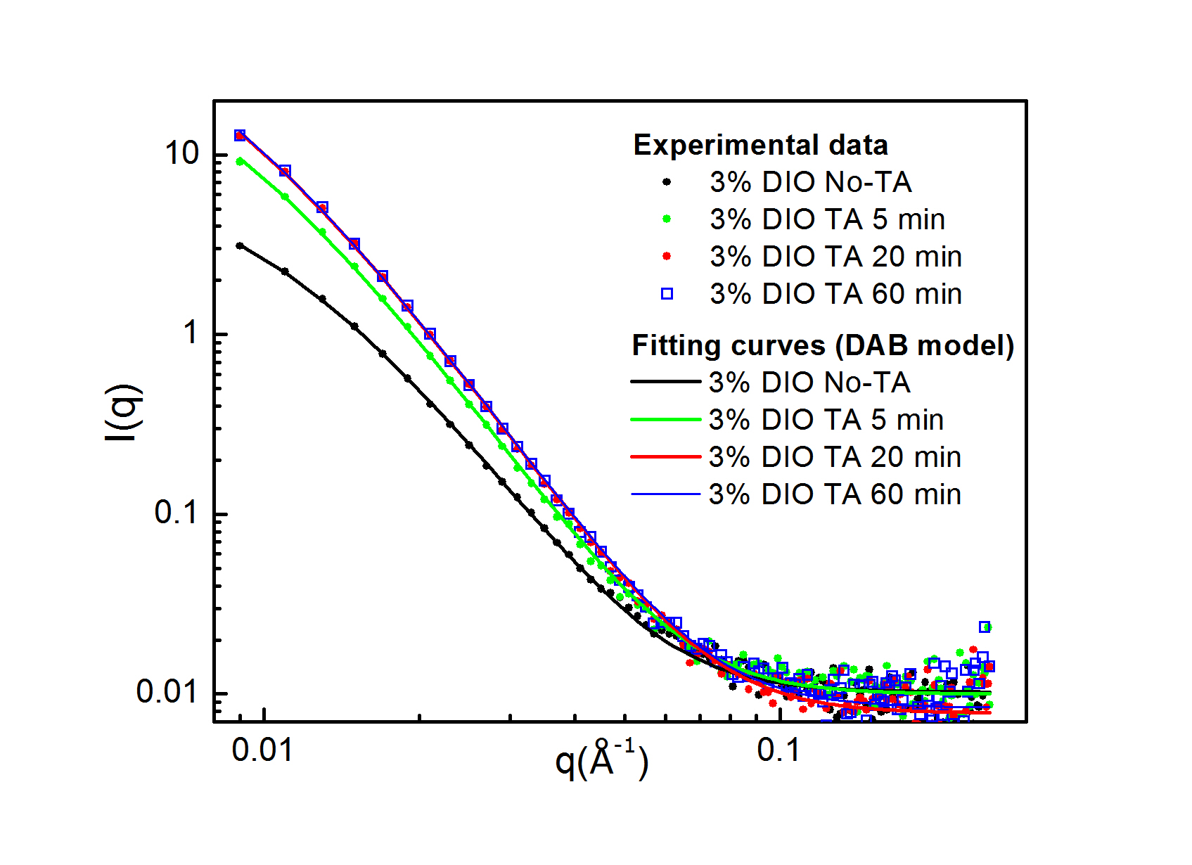
Figure 2. SANS intensity (I) as a function of scattering vector (q), relative to the system PffBT4T-2OD/PC71BM, for the non-annealed film and the film annealed for 5, 20 and 60 minutes
Observation: More examples of the successful application of SANS in the study of the bulk morphology of BHJ thin films will be reported in this website as soon as the corresponding works are accepted for publication and published on-line
PART II
Another important objective of this project consisted in contributing to a better understanding of the relationship between processing conditions, active layer morphology and device performance in polymer solar cells.
As described below, we have unravelled with an unprecedented level of detail, one of the mechanisms of action of additives in the improvement of the efficiency of BHJs. This was achieved in the study of the effect of the additive
1,8-diiodooctane (DIO) and of thermal annealing on the morphology and efficiency of PffBT4T-2OD/PC71BM devices.
Figure 3(a) below shows the chemical structure of the polymer PffBT4T-2OD. Figure 3(b) shows the structure of the OPV devices studied in this work, comprising ITO/PEDOT:PSS/Active layer/Ca/Al.
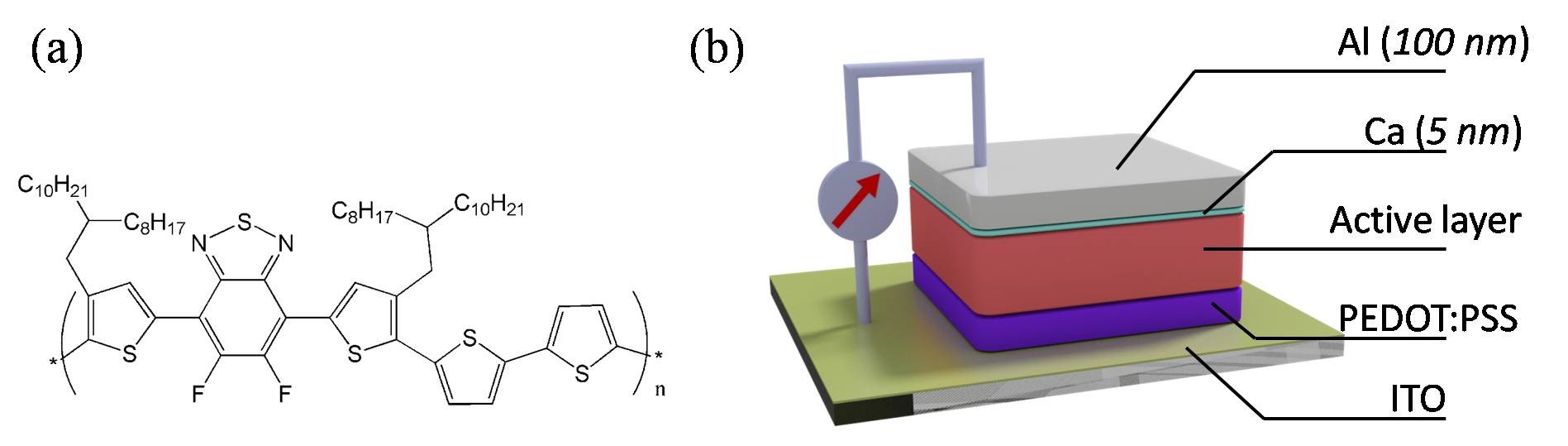
Figure 3. (a) Molecular structure of PffBT4T-2OD (b) A schematic of the device structure explored.
Figure 4(a) below shows current density-voltage (JV) curves of devices processed with DIO and then annealed for different times as well as an unannealed control. Figure 4(b) shows representative JV curves of two devices processed without DIO, one unannealed and the other annealed for 5 minutes, together with the JV curves of the corresponding devices processed with DIO as reproduced from Fig. 4(a).
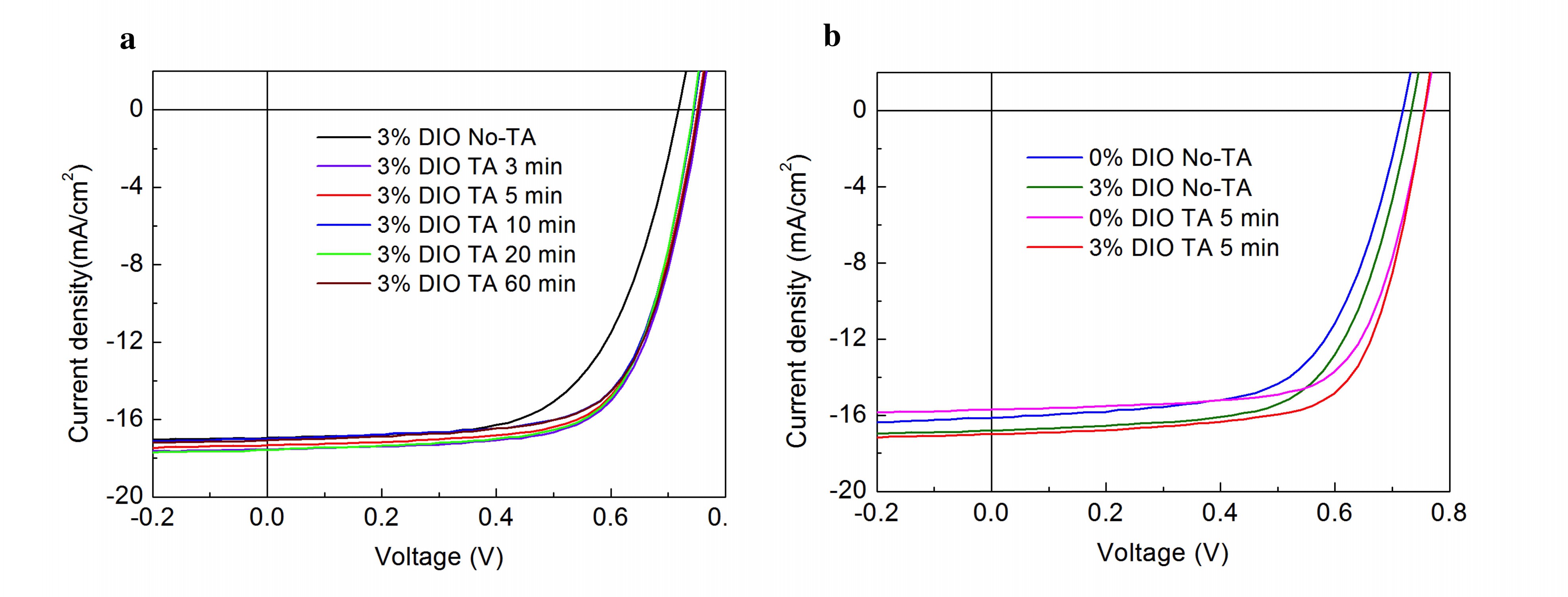
Figure 4. JV curves of devices: (a) processed with DIO and with/without different annealing time at 100 °C before cathode evaporation; (b) processed without DIO, unannealed and with 5 minutes annealing (before cathode evaporation), and corresponding devices processed with DIO.
In Figure 4(a) it can be seen that all annealed devices have a higher open-circuit voltage (Voc) and improved fill factor (FF) compared to the control. Importantly, these improvements in device metrics all occur in the initial 3 to 5 minutes of annealing, with annealing beyond this time not apparently leading to further improvements in device performance. In fact, we find that longer annealing times lead to a slight decrease in power conversion efficiency (PCE). As it can be seen in Figure 4(b), annealed devices (with and without DIO) all have very similar Voc (~0.75 ± 0.01); a value higher than the Voc of the corresponding unannealed devices (~0.72). Furthermore, devices processed with DIO have a larger short-circuit current density (Jsc) than the corresponding devices without the DIO. Therefore, while thermal annealing mainly contributes to increase Voc values, the main effect of DIO is to increase the Jsc values. The open-circuit voltage (Voc), short-circuit current density (Jsc) and the fill-factor (FF) in OPV devices are closely correlated to the nano-morphology and the hierarchical structures of the BHJ. In order to identify the origin of their enhancement, we have conducted a detailed morphological study using a number of techniques as detailed below
Figure 5 shows the variation in thickness of a BHJ film processed from a CB/DCB solvent mixture containing 3 wt% DIO measured using spectroscopic ellipsometry, as a function of time as it is annealed at 100 °C. The inset shows the same data, plotted around the initial 5 minutes for films with and without DIO, with thickness normalised to its value after 5 minutes annealing at 100 °C.
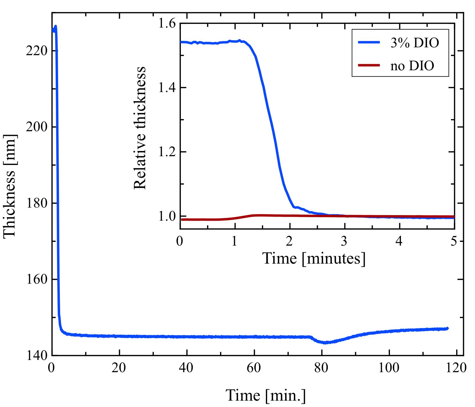
Figure 5. Dynamic data for the isothermal annealing of a PffBT4T-2OD:PC71BM blend film annealed at 100 °C. The heating stage was at 100 °C at time t = 1 minute. The inset shows a zoomed in region at the beginning showing the dramatic drop in thickness within the first minute of being at temperature.
The results clearly show that in the case of the film processed with DIO, there is a drop of > 30% in film thickness during the first 2 minutes of the annealing; a process that we attribute to the loss of DIO through evaporation. In contrast, the film that does not contain DIO undergoes a small increase in thickness, which we attribute to thermal expansion of the film. This indicates that in this film, the CB/DCB casting solvent underwent complete evaporation during spin-coating.
In Figure 6(a) we plot neutron reflectivity spectra for the OPV blend films processed with DIO for different annealing times as shown. Figure 6(b) plots scattering length density plots normal to the film surface determined from the reflectivity spectra. The different layers (silicon, PEDOT:PSS and the active layer blend) are readily identifiable due to their different scattering length densities, allowing us to determine the changes in composition within the blend layer itself.
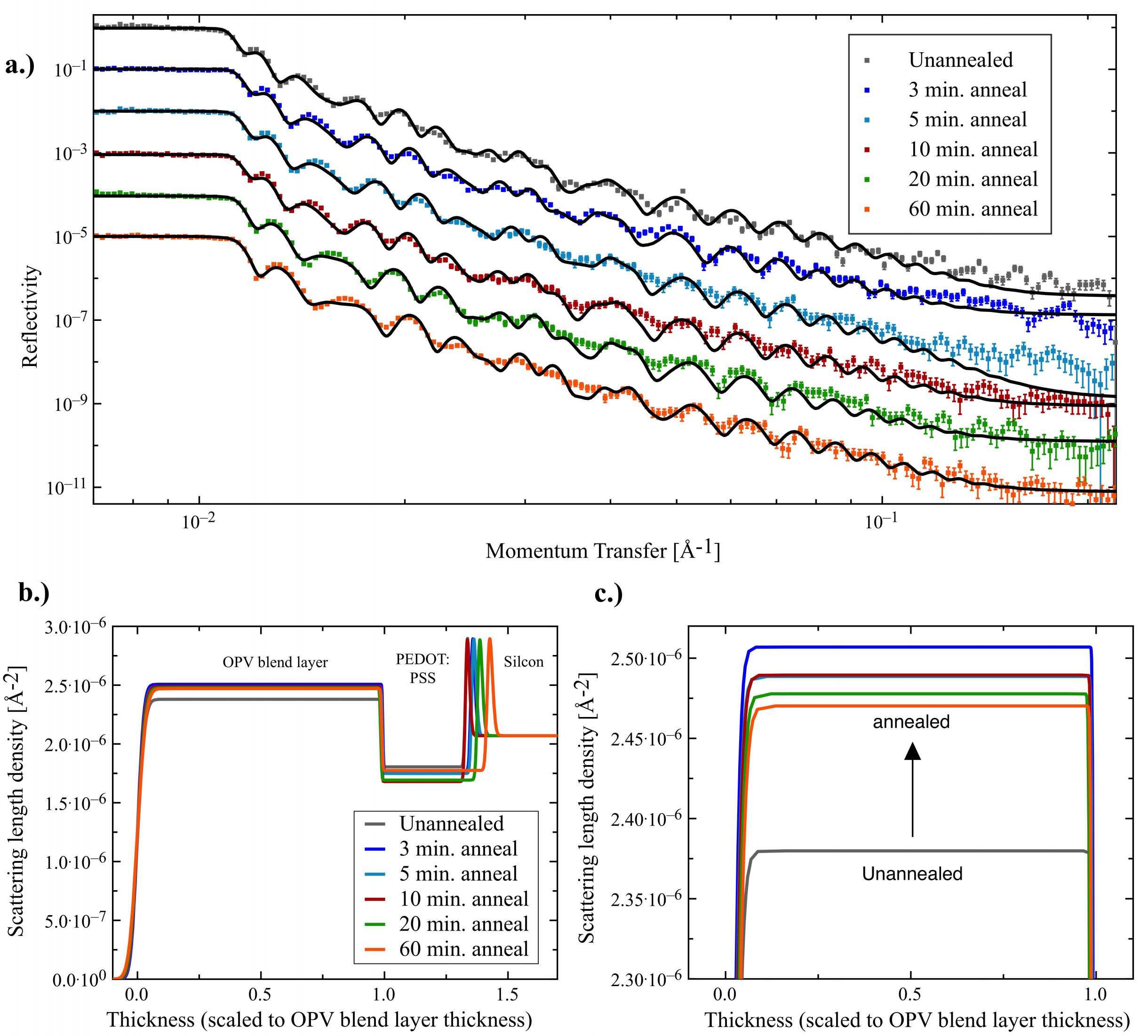
Figure 6. (a) Fitted neutron reflectivity data for a series of PffBT4T-2OD:PC71BM blend films from unannealed through annealing conditions at 100 °C for 3, 5, 10, 20 and 60 minutes; the data is offset by a decade to aid comparison; (b) The scattering length density (SLD) profiles generated from the NR fitted data. The thickness is scaled to the thickness of the OPV blend layer to aid comparisons in the profiles; (c) a zoomed in view of the change in scattering length density from the unannealed sample, showing the change in SLD upwards after thermal annealing.
By fitting the NR data, we obtain effective SLD of the unannealed blend layer and blend layer after 3 minutes annealing of 2.38x10⁻⁶ Å-2 and 2.50x10⁻⁶ Å-2 respectively. This increase in the SLD of the BHJ after 3 minutes annealing most likely results from the loss of DIO via evaporation. After longer annealing times we determine a slight drop in the SLD of the BHJ; a result we speculate might originate from aggregation of PC71BM occurring at the film surface. However, we cannot exclude difference in SLD resulting from sample-to-sample variability.
We have used ion-beam analysis (Rutherford backscattering, RBS) to explore the evaporation of DIO from the films. RBS experiments are highly sensitive to the presence of DIO as the iodine nuclei are by far the heaviest atoms in the sample and thus ion-recoils from iodine are detected at significantly higher energy than recoils from other nuclei within the film or substrate. Ion-beam experiments do not require the time-consuming sample alignment and heating ramp steps involved in ellipsometry and thus can more accurately follow the kinetics of evaporation in the earliest stages of film drying. Our ion-beam analysis measurements shown in Figure 7 suggest that thermal annealing the BHJ films at 100 °C is enough to reduce the DIO concentration through evaporation by nearly three decades in around 20 minutes, even though this temperature is well below the DIO boiling temperature (167169 °C at a base pressure of 6 mmHg).
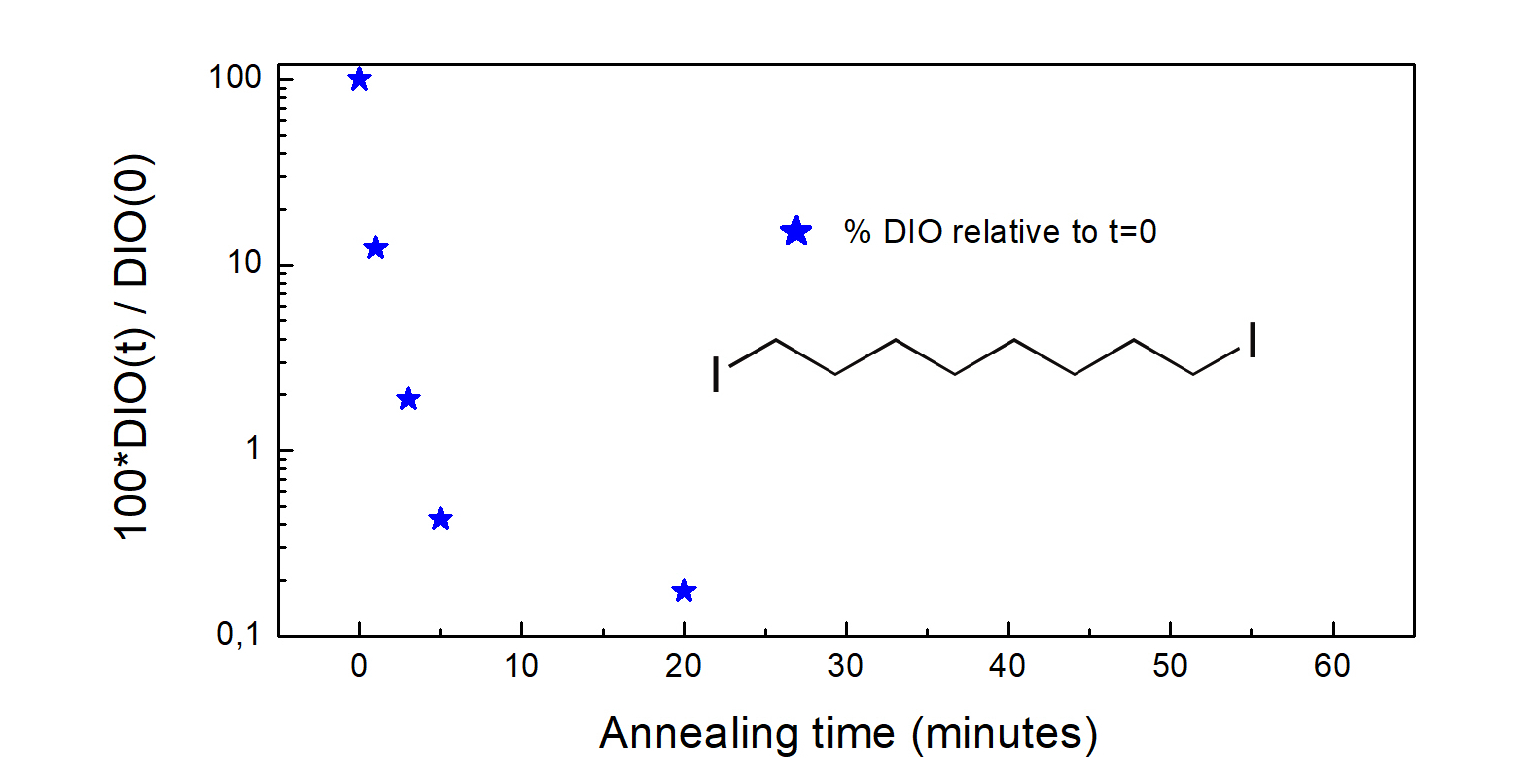
Figure 7. Removal of DIO as a function of time at 100 °C as determined using ion-beam analysis
In order to probe the bulk morphology of the film, we have used SANS and in Figure 2 above, we show SANS spectra recorded from a stack of 12 PffBT4T-2OD/PC71BM films on quartz discs (equivalent to a total dry active layer thickness of ~2.4 µm), with intensity plotted versus scattering vector, for both the annealed and unannealed samples. In SANS, the intensity is proportional to the number, size and contrast of the scattering entities in a sample, while the q-dependence of the intensity is related to their shape and local arrangement. As can be seen, there is a clear and gradual increase in scattering intensity at small q values after annealing for 5 and 20 minutes. However, samples annealed for 20 and 60 minutes show very similar scattering intensity, suggesting that after 20 minutes the system has evolved to a situation of nearly thermodynamic equilibrium.
The full data range was fitted using the Debye-Bueche (DB) or Debye-Anderson-Brumberger (DAB) model. This model calculates the scattering from a randomly distributed, two-phase system that is characterized by a single length scale - the correlation length, L - that is a measure of the average spacing between regions of two different phases (1 and 2). This function has the form: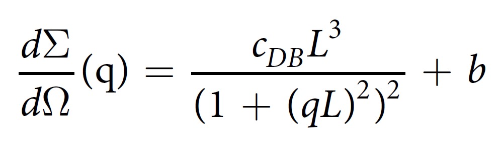
where the scaling factor CDB = 8π(Δρ)2φ1φ2 and Δρ is the neutron scattering length density difference between the phases having volume fractions of φ1 and φ2. The second term on the right hand side of the equation (b) is the background intensity that includes both instrumental and sample specific factors, i.e. the incoherent scattering intensity. As shown in Figure 2 above, the DB model gives a good description of all the data. The values obtained from the fitting for CDB and L are given in the Table below.
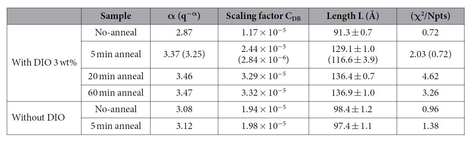
Table 1. 1st column: α values obtained by fitting the experimental data in the interval q = 0.01-0.07 Å-1 using the power law model (q- α); 2nd and 3rd columns: scaling factors (CDB) and correlation lengths (L) obtained by fitting the experimental data using the Debye-Anderson-Brumberger (DAB) model in the interval q = 0.0090.1 Å-1. The values inside the brackets for the DIO sample with 5 min thermal annealing correspond to a sample repeat prepared under similar conditions.
In Figure 8 we plot device PCE as a function of the characteristic length scale determined from SANS, where we have aggregated data from all processing conditions (namely with DIO before annealing and after annealing at 100 °C for times of 5 min, 20 min and 60 min, without DIO and without annealing and without DIO and with 5 minutes of annealing at 100 °C).
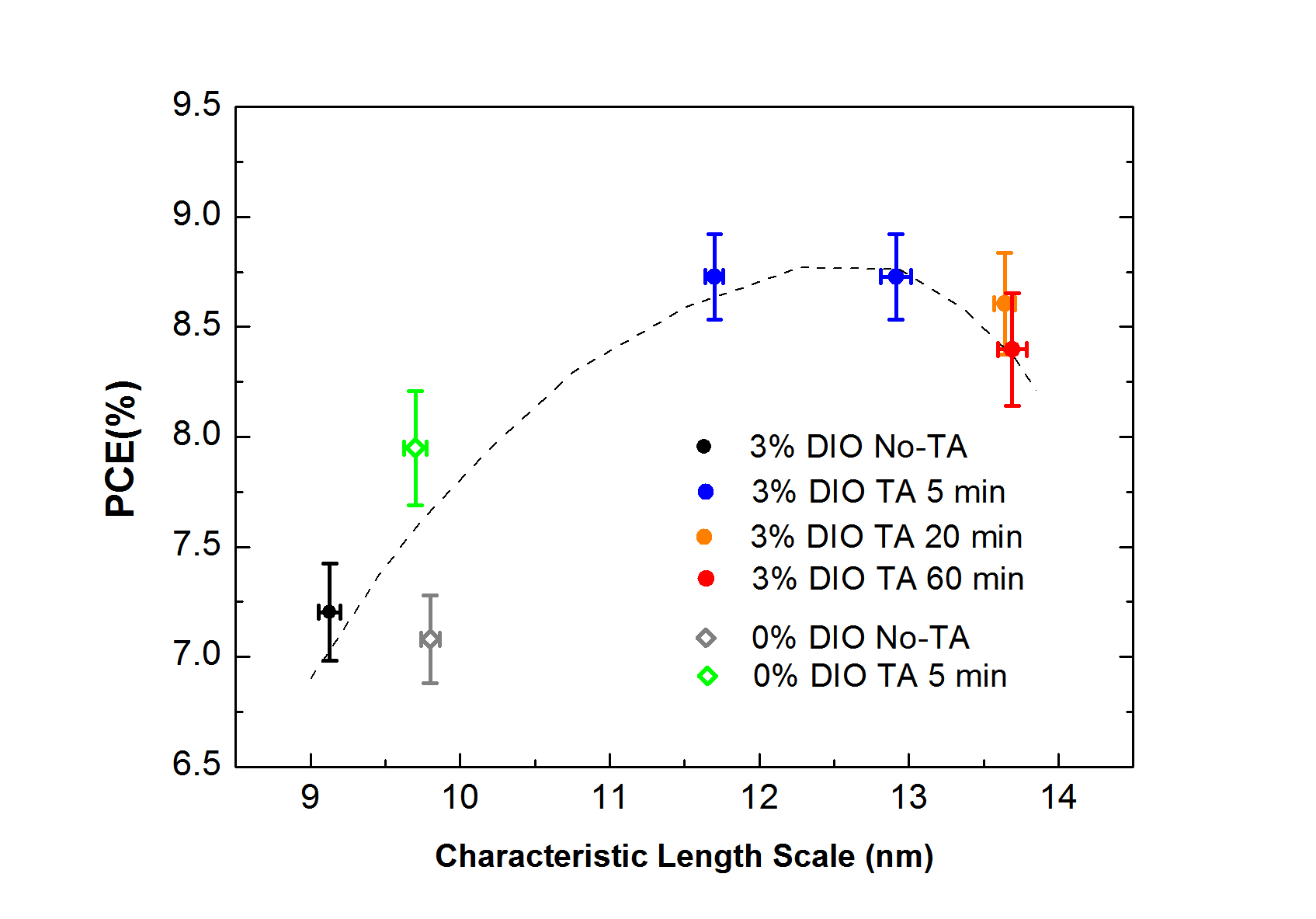
Figure 8. Correlation between PCE and characteristic length scale for samples processed in different ways, i.e. with/without DIO and with/without annealing.
In conclusion, our results strongly suggest therefore that there is an interplay between the kinetics of domain coarsening and the evaporation of DIO. Indeed, the amount of plasticizer DIO present in the film drops abruptly during annealing due to evaporation, being almost completely removed from the film after 20 minutes. On removal of the DIO, the rate of domain coarsening drops abruptly, with the final film phase morphology becoming effectively locked-in. We believe therefore that the domain size within a polymer:fullerene blend may be controllable through the selection of plasticizers having different evaporation rates, with our results providing a rational framework for the development of improved processing routes for PV-applicable BHJ materials.
Observation: More results from this project will be reported in this website as soon as the corresponding works are accepted for publication and published on-line
Publications
1. Yiwei Zhang, Andrew J. Parnell, Fabio Pontecchiani, Joshaniel F. K. Cooper, Richard L. Thompson, Richard A. L. Jones, Stephen M. King, David G. Lidzey, Gabriel Bernardo, "Understanding and controlling morphology
evolution via DIO plasticization in PffBT4T-2OD/PC71BM devices", Scientific Reports 7, 44269 (2017)
http://dx.doi.org/10.1038/srep44269
2. Yiwei Zhang, Andrew J. Parnell, Oskar Blaszczyk, Andrew J. Musser, Ifor Samuel, David G. Lidzey and Gabriel Bernardo, "Effect of Fullerene Acceptor on the Performance of Solar Cells based on PffBT4T-2OD",
Physical Chemistry Chemical Physics 20 (2018) 19023-19029
http://dx.doi.org/10.1039/C8CP02195C
3. Gabriel Bernardo, Adam. L. Washington, Yiwei Zhang, Stephen. M. King, Daniel. T. W. Toolan, Michael P. Weir, Alan D. F. Dunbar, Jonathan R. Howse, Rajeev Dattani, John Patrick A. Fairclough, Andrew J. Parnell, Does 1,8-Diiodooctane (DIO) Affect the Aggregation State of PC71BM in Solution?, Royal Society Open Science 5 (2018) 180937
http://doi.org/10.1098/rsos.180937
http://doi.org/10.5061/dryad.553t5
4. Gabriel Pérez, Gabriel Bernardo, Hugo Gaspar, Joshaniel Cooper, Francesco Bastianini, Andrew Parnell, Alan Dunbar, "Determination of the Thin Film Structure of Zwitterion Doped Poly(3,4-ethylenedioxythiophene):Poly(styrenesulfonate). A Neutron Reflectivity Study", ACS Applied Materials & Interfaces 11 (2019) 1380313811
http://doi.org/10.1021/acsami.9b02700
5. Gabriel Bernardo, Hugo Gaspar, Gabriel E. Pérez, Alec S. D. Shackleford, Andrew J. Parnell, Markus Bleuel, Adélio Mendes, Stephen M. King, Steven R. Parnell, "Impact of 1,8-diiodooctane on the morphology of organic photovoltaic (OPV) devices A Small Angle Neutron Scattering (SANS) study", Polymer Testing (2020) In Press
https://doi.org/10.1016/j.polymertesting.2019.106305
6. Gabriel Bernardo, Andrew Dennison, Richard A. L. Jones, Andrew J. Parnell, "Monitoring the removal of trapped solvent additives by thermal annealing from thin film organic photovoltaic cells", in preparation
Acknowledgements